
高压包™ 可编程混合信号矩阵,四个输出,工作电压高达13.2V,每个输出电流高达2A
SLG47105将混合信号逻辑和高压H桥式功能组合在微小的2×3mm QFN封装中。一个时间可编程(OTP)非易失性存储器(NVM)以内部逻辑,I / O引脚和宏小区的互连形式存储用户定义的解决方案。
我ntegrated dual H-Bridge/quad Half-Bridge functionality allows driving different loads up to 2A per output with up to 13.2V voltage. The SLG47105 advanced PWM macrocells provide the ability to drive multiple motors with different PWM frequencies and duty cycles. Low idle current consumption in combination with a compact size further extends the field of possible applications.
这一高度通用的设备允许多种混合信号功能的设计与高电压能力在一个微小的和热效率的集成电路。
Macrocells Overview
四个高电压、电流驱动GPO,低RDS\U开启
具有构建的两个8位PWM宏小区16字节寄存器文件
Two Oscilllators:
- 2.048 kHz oscillator
- 25 MHz oscillator
两个集成电压基准的高速通用轨对轨模拟比较器
具有积分器和模拟比较器的差分放大器
两个集成电压基准的电流检测比较器
12个组合功能宏单元:
- 三个可选的DFF/锁存器或2位LUT;
- One Selectable Programmable Pattern Generator or 2-bit LUT;
- 六个可选的DFF /闩锁或3位LUT;
- 一个可选择的管道延迟或纹波计数器或3位LUT;
- 一个可选的DFF/锁存器或4位LUT
我2串行通信宏单元
Temperature Sensor
带边缘检测器的滤波器
Programmable Delay with Edge Detector
权力On Reset (POR)
Features
Up to 13.2V High Voltage and up to 2A High Current Drive GPOs
全H桥和独立半桥控制。
灵活的8位PWMS宏小区
Constant Current Regulation
Constant Voltage Regulation
两个宽范围电源输入:
- 2.5 V (±8 %) to 5.0 V (±10 %) VDD
- 3.3 V (±10 %) to 12.0 V (±10 %) VDD2
内置保护:
- 欠压闭锁
- 过电流保护
- 热关机
我2C控制
工作温度范围:-40°C至85°C
一次性可编程非易失性存储器
低电流消耗(NA级别)
RoHS兼容/无卤素
亚博国际官网平台网址
Smart Locks and Valves
自动取款机和POS打印机
MOSFET驱动器
摄像头(视频安全、数码单反)
Toys
机器人
个人计算机和服务器
Office Equipment
个人和医疗护理设备
其他Consumer Electronics
包裹和订购
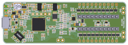
SLG47105型五:STQFN-20:(2.0 x 3.0 x 0.55 mm,0.4 mm间距)
产品标识后缀表示包装样式。
格林帕克Configurable Mixed-signal IC Introduction
GreenPak Designer软件
格林帕克Development Platform
选择正确的GreenPak
在我们的网站中查看GreenPAK视频的完整列表Training Video Library.
This product is available in one package:
SLG47105型五:STQFN-20:(2.0 x 3.0 x 0.55 mm,0.4 mm间距)
Development board selector

为GreenPAK设备提供完整的编程、仿真和测试功能。用于SLG46xxxX SKT插座套件。
与GreenPak Designer软件一起工作,GreenPak高级开发板允许设计人员:
- Program custom samples in minutes
- Test GreenPAK projects in-circuit
- 使用任何GreenPak设备开发
适用于:
- Programming
- 仿真
- 信号和逻辑发生器
Features:
- USB interface
- MacOS,Windows和Linux兼容
- 编程和仿真
- Gated expansion header for connection to external test equipment
- 集成信号和逻辑发生器
- 用于视觉指示的LED
完美的实验板和快速原型。
与GreenPAK Designer软件协同工作,GreenPAK DIP开发板允许设计师:
- Program custom samples in minutes
- Test GreenPAK projects in-circuit
适用于:
- Programming
- 仿真
Features:
- USB interface
- MacOS,Windows和Linux兼容
- 编程和仿真
- Gated expansion header for connection to external test equipment

Provides advanced emulation and testing functions for select GreenPAK devices.
Working in tandem with the GreenPAK Designer software, GreenPAK Pro Development Board allows designers to:
- Program custom samples in minutes
- Test GreenPAK projects in-circuit
- 使用Select GreenPak设备开发
适用于:
- Programming
- 仿真
- 信号和逻辑发生器
- 高速信号和逻辑发生器
- 逻辑分析仪**
Features:
- USB interface
- MacOS,Windows和Linux兼容
- 编程和仿真
- Gated expansion header for connection to external test equipment
- 我ntegrated high speed signal and logic generators
**This feature is not available at the moment and will be added through the software update
格林帕克Advanced Development Board
Provides full programming, emulation and testing functions for GreenPAK devices.
- Programming
- 仿真
- 信号和逻辑发生器
GreenPAK DIP开发委员会
完美的实验板和快速原型。
与GreenPAK Designer软件协同工作,GreenPAK DIP开发板允许设计师:
- Program custom samples in minutes
- Test GreenPAK projects in-circuit
- Programming
- 仿真
GreenPAK Pro开发委员会
Provides advanced emulation and testing functions for select GreenPAK devices.
Working in tandem with the GreenPAK Designer software, GreenPAK Pro Development Board allows designers to:
- Program custom samples in minutes
- Test GreenPAK projects in-circuit
- 使用Select GreenPak设备开发
- Programming
- 仿真
- 信号和逻辑发生器
- 高速信号和逻辑发生器
- 逻辑分析仪**
其他部件

可编程混合信号矩阵。两个电源输入:2.5 V至5.0 V和3.3 V至12.0 V. 8-GPIO,4个HV GPO,电流为每次输出最多2A,2 PWM,2 ACMP,2 CCMP,Integrator,17 LUT(最大值),15 dff /锁存器(最大),5 cnt / dly(max。)和其他宏细胞。包STQFN-20(2.0 x 3.0 mm)。
价格table:
| 数量 | 100-8,999 | 9,000-49,999 | 50,000+ |
|---|---|---|---|
| 价格 | $0.50 | $0.433 | 接触对话框 |
可编程混合信号矩阵。两个电源输入:2.5 V至5.0 V和3.3 V至12.0 V. 8-GPIO,4个HV GPO,电流为每次输出最多2A,2 PWM,2 ACMP,2 CCMP,Integrator,17 LUT(最大值),15 dff /锁存器(最大),5 cnt / dly(max。)和其他宏细胞。包STQFN-20(2.0 x 3.0 mm)。
价格table:
| 数量 | 3000-8,999 | 9,000-49,999 | 50,000+ |
|---|---|---|---|
| 价格 | $0.50 | $0.43 | 接触对话框 |

包括:SLG4SA20HV-20X30插座适配器,50 SLG47105V样品。
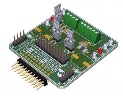
SLG47105V评估板。用于测试所有功能和大电流负载的设计。

HVPAK SLG47105演示板.
Developed for testing designs based on SLG47105 with built-in DCM, Stepper Motor and LED.

20-pin原型板。完美的实验板和快速原型。
返回结果
三周前
SLG47105型五ldle current
张贴了koen@weijand.nl.0分 15个答复在一个测试板上有一个新的裸芯片,除了VDD和I2C之外什么都没有连接。使用I2C串行调试板ext电源模拟该芯片,vcc电流达到32。3V时为6mA在按下模拟按钮之后;在移除I2C之后,电流仍然存在。它不会穿过任何针脚。
我可以在IO引脚监控HV驱动器的睡眠PIN,这是高,HV驱动器引脚都是HIGHZ。OSC也强制使用相同的网络来关闭电源。确认关闭/断电。
所有IO都是0或高,没有中途水平。当HV输出不在睡眠时但禁用时,输出引脚在轨道或GND上方0.3V。最有可能从栅极驱动电荷泵泄漏。
但是32mA去哪了?有没有可能通过不正确的编程代码来缩短一些内部代码?我是测试者?它是超级依赖的,当VDD上升时上升。
in my case the VDD and HVvdd are the same net.
感谢您的帮助。。。
三周前
一个未编程的设备似乎没有响应能力,它是否需要先编程才能使用serial调试器进行仿真?开发板仿真执行各种“轨上”信号,加上I2C。这是调试器sebds ou发出的命令,但没有来自47105V的响应。是否需要连接VDD2?
| 附件 | 大小 |
|---|---|
| i2c1stcommand.pdf. | 72.67 KB. |
三周前
the thermal pads are not connected for simplicity as the motor currents are < 100mA
三周前
another thing that I noticed is that there is a diode between VDD and VDD2 , so VDD2 is not allowed to be 0.6V lower than VDD. this is not propely reflected in the datasheet. if this 0.6V does trigger parasitic devices is not stated either.
三周前
Thank you for the feedback. Chip current consumption should be measured via GND. Could you please attach the design file, so I can take a closer look
亲切的问候
希瓦尼
两周前
a programmed chip does have the problem. It appears that I have connected two IO ports to the same voltage level as VDD , this is part of the intended design. the logic of the port is tristate or HI, so no conflict in a programmed state.
my guess is that the initiation of the chip is not properly done as it sees a conflict in the IO port halfway. that incomplete programming results in the high current state.
三周前
当我把HVVD1和2从VDD导轨上取下,然后进行模拟时,电流就消失了,同样当我把HVVD1和2连接到VDD之后。