
HV PAK™ Programmable Mixed-signal Matrix with Four Outputs with Operating Voltage up to 13.2V and up to 2A Current per Output
The SLG47105 combines mixed-signal logic and high-voltage H-bridge functionality in a tiny 2 x 3 mm QFN package. One time programmable (OTP) Non-Volatile Memory (NVM) stores user-defined solutions in the form of interconnections of internal logic, I/O pins, and macrocells.
Integrated dual H-Bridge/quad Half-Bridge functionality allows driving different loads up to 2A per output with up to 13.2V voltage. The SLG47105 advanced PWM macrocells provide the ability to drive multiple motors with different PWM frequencies and duty cycles. Low idle current consumption in combination with a compact size further extends the field of possible applications.
这个高度通用的设备允许多种多样of mixed-signal functions to be designed alongside with high-voltage capabilities within a tiny and thermally efficient IC.
Macrocells Overview
Four High Voltage, Current Drive GPOs with low RDS_ON
Two 8-bit PWM Macrocells with build-in 16-byte register file
Two Oscilllators:
- 2.048 kHz oscillator
- 25 MHz oscillator
Two High Speed General Purpose Rail-to-Rail Analog Comparators with Integrated Voltage Reference
Differential Amplifier with Integrator and Analog Comparator
Two Current Sense Comparators with Integrated Voltage Reference
Twelve Combination Function Macrocells:
- Three Selectable DFF/Latch or 2-bit LUTs;
- One Selectable Programmable Pattern Generator or 2-bit LUT;
- Six Selectable DFF/Latch or 3-bit LUTs;
- One Selectable Pipe Delay or Ripple Counter or 3-bit LUT;
- One Selectable DFF/Latch or 4-bit LUT
I2C Serial Communication Macrocell
Temperature Sensor
Filter with Edge Detector
Programmable Delay with Edge Detector
Power On Reset (POR)
Features
Up to 13.2V High Voltage and up to 2A High Current Drive GPOs
Full H-Bridge and Independent Half-Bridge Control.
Flexible 8-bit PWMs Macrocells
Constant Current Regulation
Constant Voltage Regulation
Two Wide Range Power Supply Inputs:
- 2.5 V (±8 %) to 5.0 V (±10 %) VDD
- 3.3 V (±10 %) to 12.0 V (±10 %) VDD2
Built-in Protections:
- Undervoltage Lockout
- Overcurrent Protection
- Thermal Shutdown
I2C control
Operating Temperature Range: -40 °C to 85 °C
One Time Programmable Non-Volatile Memory
Low current consumption (nA level)
RoHS Compliant/Halogen-Free
亚博国际官网平台网址
Smart Locks and Valves
ATMs and POS Printers
MOSFET Drivers
Cameras (Video Security, DSLRs)
Toys
Robotics
个人电脑和服务器
Office Equipment
Personal and Medical Care Devices
Other Consumer Electronics
Packages and Ordering
SLG47105V: STQFN-20: (2.0 x 3.0 x 0.55 mm, 0.4 mm pitch)
The product ID suffix indicates the package style.
Stay connected
Get in touch with us directly through our worldwide sales offices, or contact one of our global distributors and representatives.
Inquiries Distributors and Representatives Register for newslettersStay connected
Get in touch with us directly through our worldwide sales offices, or contact one of our global distributors and representatives.
Inquiries Distributors and Representatives Register for newslettersGreenPAK Configurable Mixed-signal IC Introduction
GreenPAK Designer Software
GreenPAK Development Platform
Choosing the Right GreenPAK
View the full list of the GreenPAK videos in ourTraining Video Library.
Stay connected
Get in touch with us directly through our worldwide sales offices, or contact one of our global distributors and representatives.
Inquiries Distributors and Representatives Register for newslettersThis product is available in one package:
SLG47105V: STQFN-20: (2.0 x 3.0 x 0.55 mm, 0.4 mm pitch)
Development board selector

Provides full programming, emulation and testing functions for GreenPAK devices. For use with SLG46xxxX-SKT sockets kits.
Working in tandem with the GreenPAK Designer software, GreenPAK Advanced Development Board allows designers to:
- Program custom samples in minutes
- Test GreenPAK projects in-circuit
- Develop using any GreenPAK device
Suitable for:
- Programming
- Emulation
- Signal and Logic Generators
Features:
- USB interface
- MacOS, Windows and Linux compatible
- Programming and Emulation
- Gated expansion header for connection to external test equipment
- Integrated signal and logic generators
- LEDs for visual indication
Perfect for breadboarding and fast prototypes.
Working in tandem with the GreenPAK Designer software, GreenPAK DIP Development Board allows designers to:
- Program custom samples in minutes
- Test GreenPAK projects in-circuit
Suitable for:
- Programming
- Emulation
Features:
- USB interface
- MacOS, Windows and Linux compatible
- Programming and Emulation
- Gated expansion header for connection to external test equipment

Provides advanced emulation and testing functions for select GreenPAK devices.
Working in tandem with the GreenPAK Designer software, GreenPAK Pro Development Board allows designers to:
- Program custom samples in minutes
- Test GreenPAK projects in-circuit
- Develop using select GreenPAK device
Suitable for:
- Programming
- Emulation
- Signal and Logic Generators
- High Speed Signal and Logic Generators
- Logic Analyzer**
Features:
- USB interface
- MacOS, Windows and Linux compatible
- Programming and Emulation
- Gated expansion header for connection to external test equipment
- Integrated high speed signal and logic generators
**This feature is not available at the moment and will be added through the software update
GreenPAK Advanced Development Board
Provides full programming, emulation and testing functions for GreenPAK devices.
- Programming
- Emulation
- Signal and Logic Generators
GreenPAK DIP Development Board
Perfect for breadboarding and fast prototypes.
Working in tandem with the GreenPAK Designer software, GreenPAK DIP Development Board allows designers to:
- Program custom samples in minutes
- Test GreenPAK projects in-circuit
- Programming
- Emulation
GreenPAK Pro Development Board
Provides advanced emulation and testing functions for select GreenPAK devices.
Working in tandem with the GreenPAK Designer software, GreenPAK Pro Development Board allows designers to:
- Program custom samples in minutes
- Test GreenPAK projects in-circuit
- Develop using select GreenPAK device
- Programming
- Emulation
- Signal and Logic Generators
- High Speed Signal and Logic Generators
- Logic Analyzer**
Other components

Programmable Mixed-signal Matrix. Two Power Supply Inputs: 2.5 V to 5.0 V and 3.3 V to 12.0 V. 8-GPIO, 4 HV GPO with current up to 2A per Output, 2 PWM, 2 ACMP, 2 CCMP, Integrator, 17 LUTs (max.), 15 DFF/LATCH (max.), 5 CNT/DLY (max.) and other Macrocells. Package STQFN-20 (2.0 x 3.0 mm).
Price table:
| Qty | 100-8,999 | 9,000-49,999 | 50,000+ |
|---|---|---|---|
| Price | $0.50 | $0.433 | Contact Dialog |
Programmable Mixed-signal Matrix. Two Power Supply Inputs: 2.5 V to 5.0 V and 3.3 V to 12.0 V. 8-GPIO, 4 HV GPO with current up to 2A per Output, 2 PWM, 2 ACMP, 2 CCMP, Integrator, 17 LUTs (max.), 15 DFF/LATCH (max.), 5 CNT/DLY (max.) and other Macrocells. Package STQFN-20 (2.0 x 3.0 mm).
Price table:
| Qty | 3000-8,999 | 9,000-49,999 | 50,000+ |
|---|---|---|---|
| Price | $0.50 | $0.43 | Contact Dialog |

Included are: SLG4SA20HV-20x30 socket adapter, 50 SLG47105V samples.
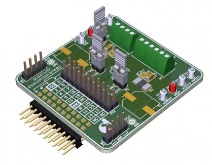
Evaluation Board for SLG47105V. Developed for testing designs with all features and high current loads.

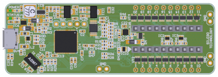
HVPAK SLG47105 Demo Board.
Developed for testing designs based on SLG47105 with built-in DCM, Stepper Motor and LED.

20-pin DIP Proto Board. Perfect for breadboarding and fast prototypes.
Stay connected
Get in touch with us directly through our worldwide sales offices, or contact one of our global distributors and representatives.
Inquiries Distributors and Representatives Register for newsletters
Back to results
1 month ago
SLG46517M PFET Power Switch
Posted byYuseungho20 points 3 repliesDear,
I'm using the device SLG46517M which has two P-FET power switches. Now, I'm testing the device in emulation mode.
Here I attach my simplified design of the circuit.
The problem is that when the switch is off, the Vout node has too large spike and the spike discharges very slowly.
As a result, when it's off, it reaches almost twice the input voltage (~920mV with 500mV input). The load side now only has a fixed resistor which is 2Mohm just for test.
(I also attach the waveform)
When the switch is on, it outputs properly with the input voltage of 500mV.
As you can see, FSM(ASM) turns on OSC0 in GPAK when the condition is met, and the OSC0 triggers the PFET with 25kHz switching frequency.
I could not figure out what the problem is. I'd really appreciate if you could share your opinions.
Thank you.
Regards,
Seungho Yu
| Attachment | Size |
|---|---|
| simple circuit architecture | 111.7 KB |
| oscilloscope waveform | 223.86 KB |
1 month ago
Thank you for your answer.
Would you please tell me your email?
Because the design file might be personal, I'd like to send you by email.
Thanks.
1 month ago
I think the reason why the voltage discharges slowly is load resistor has too large resistance, which caused too high RC time constant.
I changed the load resistor from 2Mega ohm to 100 ohm, and find it shows reasonable waveform.
But I have another problem now.
According to the datasheet of SLG46517M, PFET has minimum input voltage of 300mV.
But I found that to toggle the PFET on/off, input should be larger than about 700mV(experiment result).
When the input is larger than 300mV and small than certain value, PFET cannot outputs properly (different from that input voltage, around 50mV, almost no signal).
The design has not changed, it's same as before.
Please tell me your email, then I would send you my design file.
I look forward to hearing from you.
Thank you.
1 month ago
Hi Seungho Yu,
Thank you for reaching out. Could you please share your GPAK design file (.gp) so I can look into the problem?
Best Regards
Shivani